Update: My first printed circuit board doesn’t work – to see how it all when wrong look here.
My first printed circuit board has just been designed. I’ve been creating a couple of circuits now on a breadboard, but each time I wanted to try something else I would either have to dismantle the circuit to reuse the breadboard, or buy another breadboard (I have 3 now).
Sure I can always put the circuit on a prototype board or strip board, but I find they tend to get a little messy and they aren’t as neat.
To try out this workflow I thought I’d do something really simple to start with.
I will be sending off the design to be manufactured rather than etch my own board. It gives it a professional look and you don’t have to deal with usage and storage of corrosive chemicals.
Here are the steps I used to create my printed circuit board. Hopefully it can be helpful for someone else wanted to give it a try.
Creating the schematic

I created my schematic using the EagleCAD software. The ‘light’ version is free for hobby use and it works on my mac.
The circuit is just a simple 555 timer that flashes 2 LEDs. I think the secret to learning and testing a new workflow is to keep things simple. Remember that this is my ‘helloworld’ of a printed circuit board. Don’t judge me.
Breadboard the circuit
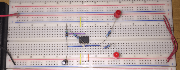
It is important to test out your circuit by building it on a breadboard first. This allows you to swap out components and change your circuit around much easier. It also saves you time and more importantly money as it costs money to manufacture a printed circuit board externally and you want to make sure there are no mistakes.
Design the Printed Circuit Board

I designed my PCB Layout using EagleCAD. This is my first ever printed circuit board design, so there are probably some things wrong with it. I’ve got a ground plane for the bottom later, and a power plane for the top layer. I managed to route all the nets on a single top layer. If anyone is interested then I’ll post up my source files.
Upload to a PCB Manufacturer
I took the final board file and uploaded to a PCB Manufacturer. I’m using OSHPark.com as I can simply upload the Eagle .brd file without messing with Gerber files that most other manufacturers use. Perhaps in the future I’ll pick a different Manufacturer (suggestions anyone?).
OSHPark.com also seems to be reasonably priced given the size of the board I created (1″ squared = $5USD for a 2 layer design), and you get 3 boards for your trouble (some places want a minimum of 100 boards – who wants 100 x 555 flasher circuits?)
Now we wait…
Now that the board has been uploaded and approved I now need to wait until it gets manufactured, and delivered to me. From the website I’m estimating about 2 weeks. When it shows up I’ll take a few photos and comment on how awesome (or crap) it is.
While there is a bit of a wait, it saves me having to deal with the messy chemicals and cleanup if I was etching my own printed circuit board.
I’m rather excited to see how it turns out – Let the waiting begin…